 Over the last decade, CMOS Image Sensor (CIS) technology has made impressive progress. Image sensor performance has dramatically improved over the years, and CIS technology has enjoyed great commercial success since the introduction of mobile phones using onboard cameras. Many people, including scientists and marketing specialists, predicted 15 years earlier that CMOS image sensors were going to completely displace CCD imaging devices, in the same way that CCD devices displaced video capture tubes during the mid-1980’s. Although CMOS has a strong position in imaging today, it has not totally displaced CCD devices. On the other hand, the drive into CMOS technology has drastically increased the overall imaging market. CMOS image sensors have not only created new product applications, but have also boosted the performance of CCD imaging devices as well. In this paper, we describe the state-of-the-art in CMOS image sensor technology and discuss future perspectives.
Image Sensor Definition and Uses
An image sensor is an electronic device that converts an optical image into an electronic signal. The method of conversion varies by the type of image sensor.
- An “analog” CCD performs photon-to-electron conversion
- A “digital” CMOS Image Sensor (CIS) performs photon-to-voltage conversion
Image sensors are used in digital cameras and imaging devices to convert light received from a camera or imaging device into a digital image.
CIS vs. CCD
Today, there are two different technologies for capturing images digitally (Fig.1):
- Charged Coupled Devices (CCDs) are linear sensors, with an output directly related to the number of photons received
- Complementary Metal Oxide Semiconductor (CMOS, or CIS for CMOS Image Sensor) is a newer, parallel readout technology
Both types of imaging devices convert light into electrons (or an electric charge) that can be subsequently processed into electronic signals. CCDs are designed to move charges from pixel to pixel until they reach amplifiers that are present in the dedicated readout area. CMOS Image Sensors integrate amplification directly in the pixel. The more advanced CIS technology provides a parallel readout architecture, where each pixel can be addressed individually or read out in parallel as a group (see Figure 1).
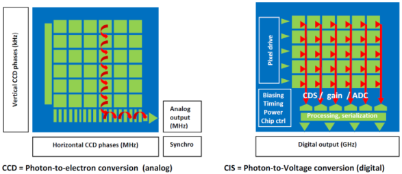
Fig. 1: CCD = Photon-to-Electron (analog) conversion (left) and CIS = Photon-to-Voltage (digital) conversion (right)
CMOS sensors are much less expensive to manufacture than CCD sensors. Digital cameras have become extremely common and inexpensive, due to the decrease in pricing of newer image sensors.
In Table 1, we show the main differences between CCD and CMOS architectures. Each has unique strengths and weaknesses, providing advantages (shown in green color) in different applications.
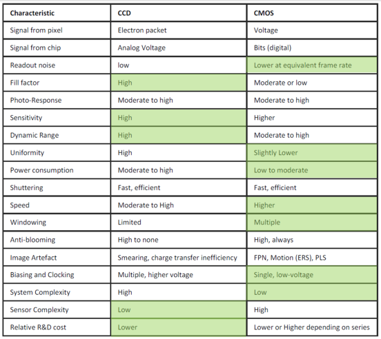
Table 1: CCD & CMOS architecture comparison (Source: e2V)
Key Components in CIS
There are four main components in a CMOS image sensor (see Figure 2):
- Photodiode (PD)
- Pixel design
- Color filter (CF)
- Microlens
The photodiode (PD) is used to capture light, with PIN diodes or Shallow PN junction devices commonly used for this purpose. The most widely implemented Pixel Design is known as an “Active Pixel Sensor” (APS). Three to six transistors are commonly used, and they provide gain or buffer the pixel from large column capacitance. The color filter is used to separate out the red, green and blue (RGB) components of reflected light. And finally, the microlens gathers light from the inactive portion of the CIS and focuses it down to the photodiode. The microlens typically has a spherical surface and a webbed lens.
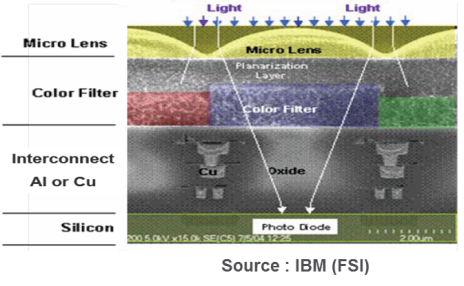
Fig. 2: Key components in CIS (Source: IBM, FSI)
CIS Performance Parameters
There are many parameters that can be used to evaluate the performance of an image sensor. We can classify these parameters using three main metrics:
- Pixel Layout : pixel count, pixel pitch, pixel fill factor
- Pixel Physics : quantum efficiency, well capacity, dynamic range, conversion gain, dark current
- Pixel Readout: signal to noise ratio, frame rate, percentage of linearity, power consumption, bit depth, modulation transfer function, shutter efficiency
BackSide Illumination (BSI) vs. FrontSide Illumination (FSI) Technologies
Advanced CMOS Image Sensor manufacturers are seeking new architectures in order to decrease pixel size while maintaining or enhancing electro-optical performance. Smaller pixels typically result in higher resolution, smaller devices, and lower power and cost. Ideally, any new CIS architecture that shrinks the pixel size should not degrade performance or image quality. One newer CIS architecture, BackSide Illumination (BSI) technology, is a promising alternative to the commonly used FrontSide Illumination (FSI) technology (see Figure 3).
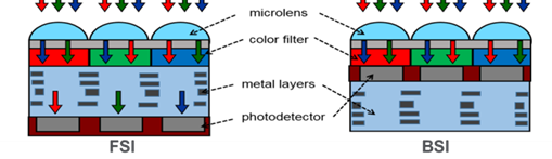
Fig. 3: FSI vs. BSI
BSI technology involves turning the image sensor upside down and applying color filters and micro lenses to the backside of the pixels, so that the sensor can collect light through the backside. BSI has a deep photo-diode and short optical path, leading to a higher Quantum Efficiency (1) (QE) and Lower Crosstalk (2) (see Figure 4).
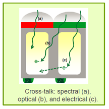
Fig. 4: Crosstalk
(1) QE = the percentage of photons that are converted into electrons
(2) Electrical Crosstalk = diffusion of electrical charge (electrons or holes depending upon the pixel type) between adjacent pixels. It occurs in silicon materials due to the underlying electrical mechanisms (diffusion and drift)
BSI Process Flow
A number of process steps are required to produce a CMOS image sensor using BackSide Illumination architecture. Diagrams describing two different BSI process flows, Si-Bulk (Figure 5) and SOI (Figure 6), are shown below:
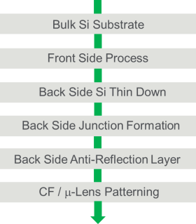
Fig. 5: BSI Si-Bulk Simplified Process
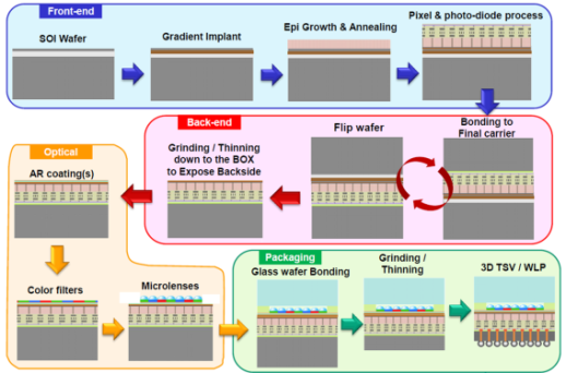
Fig. 6: BSI SOI Process Flow (Source: Yole)
Global Shutter (GS) vs. Rolling Shutter (RS) for CIS
“Rolling Shutter” (RS) is a technical term referring to the way that an image sensor scans an image. If the sensor employs a RS, this means that the image is scanned sequentially, from one side of the sensor (usually the top) to the other side, on a line by line basis. Ordinary, a CMOS image sensor operates in RS mode in which exposure and shutter operation is executed row by row (or line by line). In contrast, “Global Shutter” (GS) is a technical term referring to sensors that can scan the entire area of an image simultaneously. In a GS sensor, the image is captured simultaneously using all pixels. The GS architecture includes a memory structure and additional MOS transistors to provide additional functionality. Today, most CIS imagers have adopted GS mode to avoid distortion and artifacts such as parasitic light sensitivity (see Figure 7). CMOS image sensors using GS functionality are used in a variety of areas, including broadcasting, automotive, drone and surveillance applications.
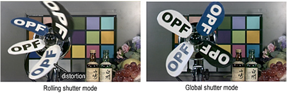
Fig. 7: Rolling (left) vs. Global (right) Shutter Modes
3D Stacked CIS
The growth of mobile phones is the primary driver for the CIS unit shipment increase over the last 5 years. As CIS market revenue has grown, so has R&D spending and patent filings. This effort has resulted in advanced mobile camera systems containing new technologies such as:
- Phase detection pixel arrays (PDPA) for fast autofocus (AF)
- ~1 µm generation pixels with improved low-light sensitivity
- Advanced chip-stacking, featuring a BSI CIS wafer joined with an image signal processor (ISP) wafer
- Video recording up to 4K
A 3D stacked image sensor consists of a BSI image sensor die, face-to-face stacked on a logic die. The motivation to invest in stacked chip CIS development has been somewhat varied depending upon the manufacturer, but can be summarized as:
- Adding functionality
- Decreasing form factor
- Enabling flexible manufacturing options
- Facilitating optimization for each die in a 3D stack
Sony announced the world’s first stacked chip CIS camera system for consumer electronics in 2012, and 8 MP ISX014 stacked chips were found in a tablet computer by early 2013. The first generation chips employed via last TSVs to connect pads from the Sony-fabricated, 90 nm CIS die to landing pads on a Sony fabricated, 65 nm generation ISP (source: Chipworks). Sony’s 13 MP IMX214 second generation stacked CIS chips were fabricated similarly using its 90/65 nm (CIS/ISP) technology generation, and were included in the iPhone6/6s during 2014. More recently (February 2017) Sony announced a 3 layer CIS device including a Top Layer BSI Sensor or CIS Photodiodes, a Mid Layer DRAM Cell Array and a Bottom Layer Logic as ISP (Figure 8). It’s a 23MP image sensor with a 1um x 1um pixel size that uses a new hybrid bonding structure (while the conventional structures are TSV like). Sony also announced its first three-layer, 960 fps camera with Sandwich-Stacked DRAM in May 2017.
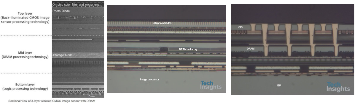
Fig. 8: Sony 3 stacked layer CIS Device (Sources: ISSCC 2017 & TechInsights)
3D Stacked CIS History
In Table 2, we present a summary of 3D stacked CIS history (source: www.3DIC.org). One can clearly see that technology moved from oxide bonding + via last TSV stacking technology to hybrid bonding, and more recently to sequential 3D integration. Researchers at National Nano Device Laboratories and National Tsinghua University, Taiwan, recently demonstrated a monolithic 3D image sensor. They sequentially fabricated a monolayer (<1nm) TMD (Transition Metal Dichalcogenide) phototransistor array, using CVD-grown MoS2 transferred onto top of a 3D logic/memory hybrid 3D IC with high density interconnects.
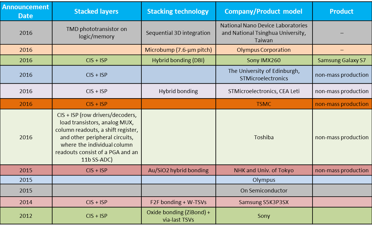
Table 2: Stacked CIS History (from www.3DIC.org)
CIS Technology/Market/Players Today and Tomorrow
The roadmap for future CIS technology adoption is fueled by three constraints or drivers:
- Size (3 dimensions, X, Y and Z of the camera module),
- Image quality (resolution, low light performance, focus (AF) and stabilization (OIS)) and
- Functionality (slow-motion video, image analysis, motion control)
BSI, 3D Stacked BSI, 3D Hybrid as well as 3D Sequential Integration are all key technologies that will affect future CIS technology adoption.
The competitive landscape in the CIS market has greatly changed over the years. Sony is a market, production and technology leader. Omnivision and Samsung have remained strong, and new players like Galaxycore and Pixelplus are emerging. Meanwhile, the Integrated Device Manufacturing (IDM) model has been a great source of strength for Canon and Nikon, who have both weathered the slow-down in digital still-cameras. As for Panasonic, it has created a joint venture with Tower Jazz to aid in its search for volume in higher-end imaging applications.
Today, the CIS industry is driven by mobile and automotive applications. Innovation in smartphone cameras will continue, even though competition in this high-volume application is intense. CIS manufacturers are being forced to integrate more and more functionality into mobile cameras (see Figure 9) in order to stay competitive.
![]()
Fig. 9: Transformation of Mobile Camera Function (Source: Yole)
Smartphone applications are leading in CIS market share, but many other applications are going to be part of CIS’ future growth. Many IDMs and fabless companies are developing chips for emerging, higher margin imaging applications such as automotive, security, medical, and other areas. Great opportunities are emerging in these applications, propelling market and technology efforts of both new and existing suppliers. These emerging opportunities are driving technology from mobile imaging to other growth areas, and we may see a shift from using vision for imaging to using vision for sensing and other interactive applications.
Was this helpful?
7 / 0
